
Highlights
- Samsung Foundry rebrands 2nd generation 3nm technology to SF2.
- Move aimed at simplifying nomenclature and boosting market stance.
- Contract revisions initiated for customers due to renaming.
- SF2 technology set for production in the second half of 2024.
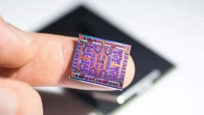
Samsung Foundry has initiated a significant rebranding of its advanced process technology.
This rebranding strategy involves transitioning the name of its 2nd generation 3nm-class fabrication technology from SF3 to SF2, aligning its naming convention more closely with industry standards, and positioning itself against rivals like Intel Foundry.

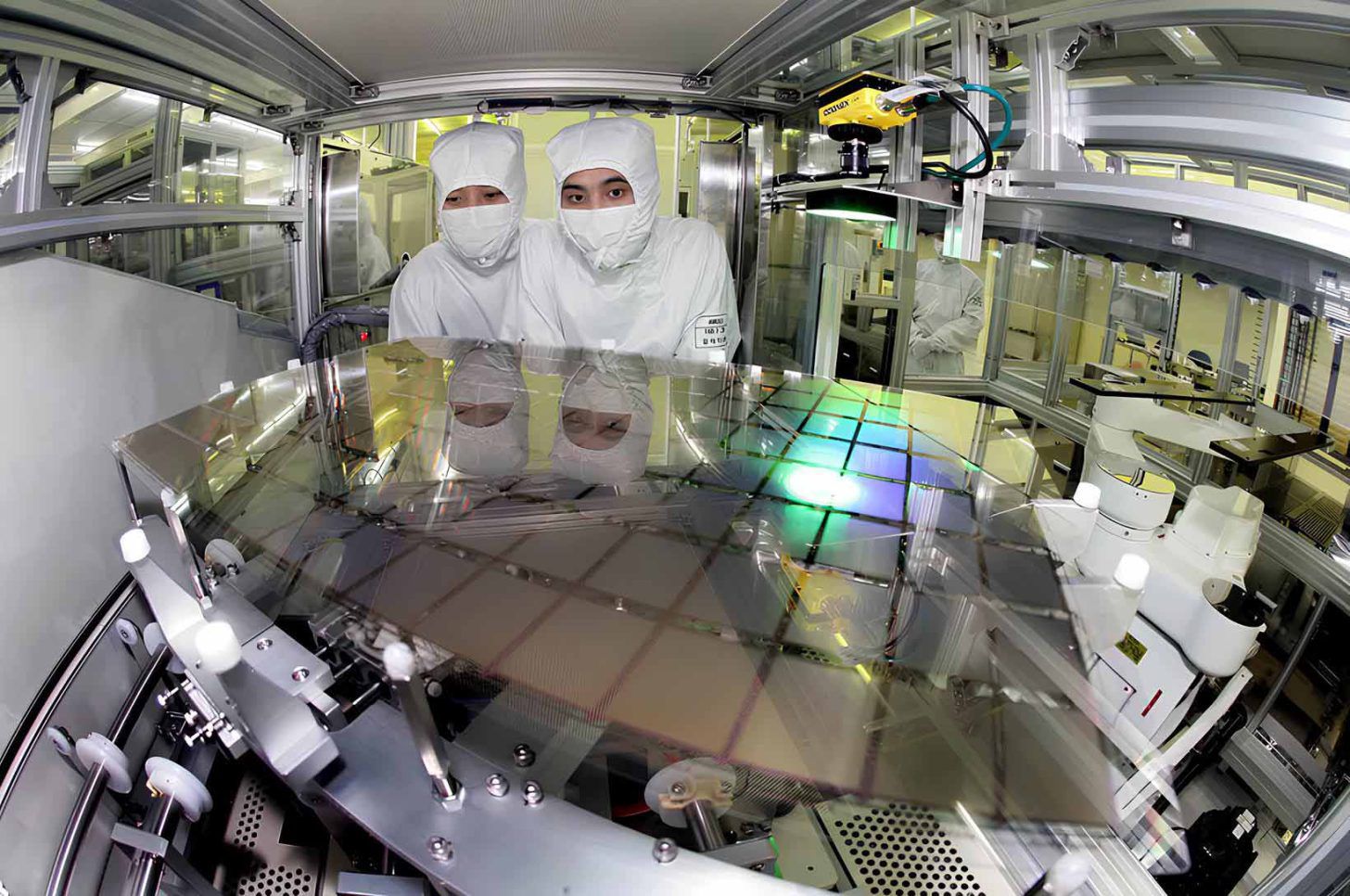
Samsung has been at the forefront of chip manufacturing for a long time now and it seems that it is puting a motion its next plan to further bolster its market positioning.
Renaming to Bolster Market Position
Korean Publication ZDNet reports that this rebranding effort could be Samsung’s attempt to streamline its process nomenclature and enhance its competitive stance, especially in light of Intel Foundry’s upcoming Intel 20A production node, a 2nm-class technology, set to debut later this year.
Samsung’s process technology roadmap, revealed in late 2022, highlights a progression through various nodes, including SF3E, SF4P, SF3, SF4X, SF2, SF3P, SF2P, and SF1.4.
The change from SF3 to SF2, communicated to customers since early 2024, necessitated contract revisions for those committed to utilizing the SF3 production node.

“We were informed by Samsung Electronics that the 2nd generation 3nm [name] is being changed to 2nm,” shared a source with ZDNet, highlighting the contractual adjustments required to accommodate this naming shift.
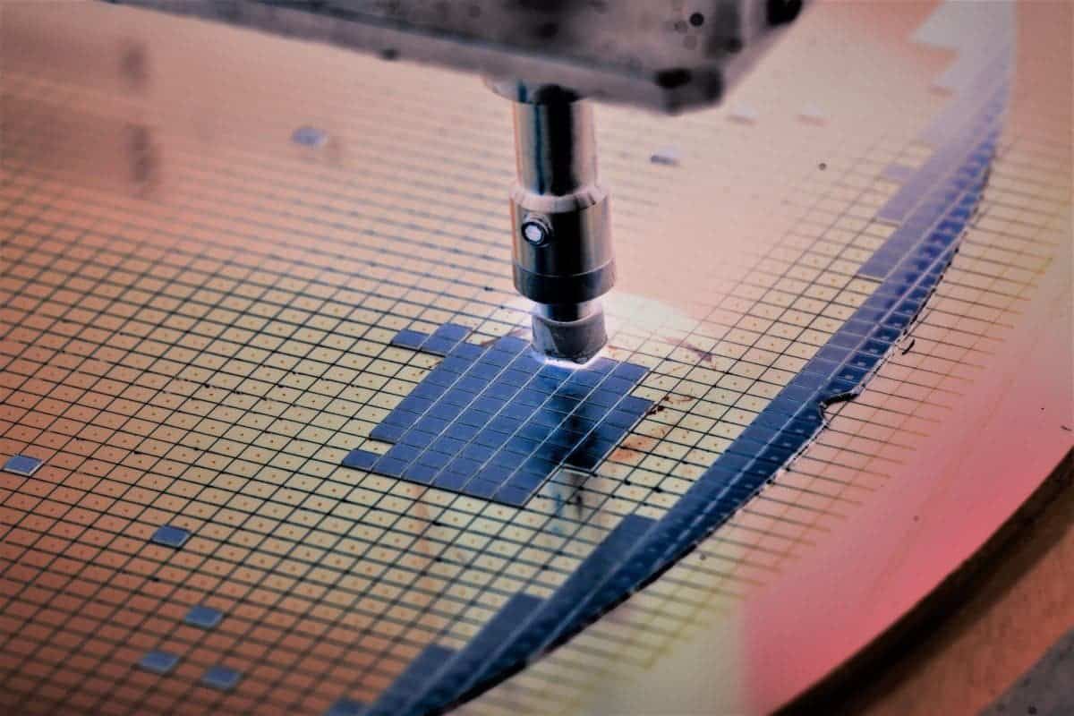
Despite the change in designation, Samsung’s commitment to innovation remains steadfast, with plans to commence chip production using the newly termed SF2 technology by the second half of 2024.
Technological Implications and Future Roadmap
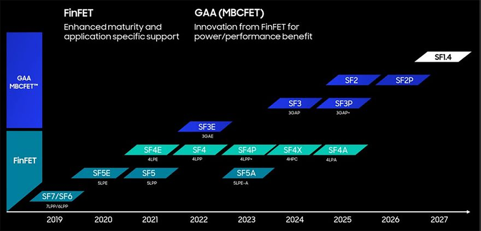
Samsung’s SF2 technology, originally known as SF3, incorporates gate-all-around (GAA) transistors, specifically Multi-Bridge-Channel Field Effect Transistors (MBCFET).
“Samsung Electronics’ second-generation 3nm (2nm) process design kit (PDK) has been released, so if Samsung rushes into mass production this year, they will be well-positioned to do so. As for the specific mass production time, it depends largely on customer requirements” said a semiconductor insider to ZDNet.
Notably, the SF2 technology does not feature a backside power delivery network (BSPDN), positioning it at a competitive disadvantage relative to Intel’s 20A process, which integrates both GAA transistors and BSPDN for enhanced performance and energy efficiency.
FAQs
Why did Samsung Foundry rename its 3nm-class technology to SF2?
Samsung Foundry’s decision to rename its 3nm-class technology to SF2 is part of a strategic effort to simplify its process nomenclature and strengthen its position against competitors, particularly Intel Foundry.
What implications does the renaming have for Samsung Foundry’s customers?
Customers who had contracts for the SF3 production node were required to revise their agreements to reflect the change to SF2, indicating a seamless transition in naming without altering the underlying technology.
When will Samsung start manufacturing chips using the SF2 technology?
Samsung plans to begin chip production using the newly named SF2 technology in the second half of 2024, following its rebranding initiative.
Does the SF2 technology have any competitive disadvantages?
While the SF2 technology incorporates advanced gate-all-around (GAA) transistors, it lacks a backside power delivery network (BSPDN), putting it at a competitive disadvantage compared to Intel’s 20A process technology.
Will there be further name changes in Samsung Foundry’s technology roadmap?
Given the recent renaming of SF3 to SF2, there is speculation that other nodes in Samsung Foundry’s technology roadmap might also undergo renaming to maintain consistency and clarity.
Also Read: Samsung’s Exynos 2500 Could Be a Deca-Core Chipset and 2nd Gem 3nm Fabrication
Also Read: Qualcomm Could Partner with Samsung for next year’s 2nm Snapdragon 8 Gen 5 Chipset