Highlights
- Intel aims to create a trillion transistor chip by 2030, challenging Moore’s Law.
- Introduction of “Super Moore’s Law” for accelerated transistor count growth.
- Collaboration with TSMC and Samsung Foundry for advanced 2nm technology.
- Significant economic shifts with rising costs in chip manufacturing.
Intel is aiming to redefine the boundaries of chip development with an ambitious goal to create a chip containing a trillion transistors by 2030.
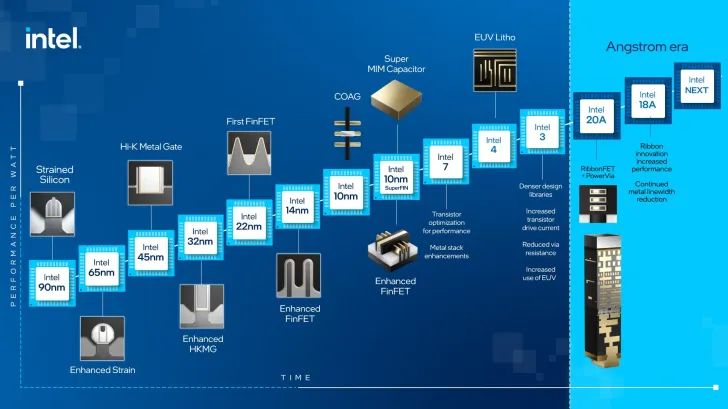
This objective marks a significant leap from the current trends dictated by Moore’s Law, which has been the guiding principle of the semiconductor industry since its coining by Intel and Fairchild Semiconductor.
Originally, Moore’s Law suggested the doubling of transistor counts every year, but over time, this pace slowed down.
The industry began to witness a doubling approximately every three years.
Despite this deceleration, Intel’s CEO, Pat Gelsinger, envisions a future where the company not only keeps pace with Moore’s Law but surpasses it by 2031.
Introducing “Super Moore’s Law” or “Moore’s Law 2.0”
As per Tom’s Hardware, Gelsinger, during a talk at the Manufacturing@MIT symposium, introduced the concept of “Super Moore’s Law” or “Moore’s Law 2.0,” emphasizing a more aggressive growth in transistor counts.
This new vision aims to accelerate the pace of technological advancement, pushing the limits of chip miniaturization and power.
To achieve this remarkable feat, Intel is not alone.
It plans to collaborate with industry giants like TSMC and Samsung Foundry, who will play a crucial role in developing these new chips, leveraging advanced 2nm node technology.
Intel is not alone in this, as even companies like Qualcomm are transitioning to TSMC and Samsung Foundry for their chip manufacturing needs.
Innovations Driving the Trillion-Transistor Vision
The task to get to a trillion transistors is not an easy one. Several key innovations are pivotal to Intel’s chip ambition:
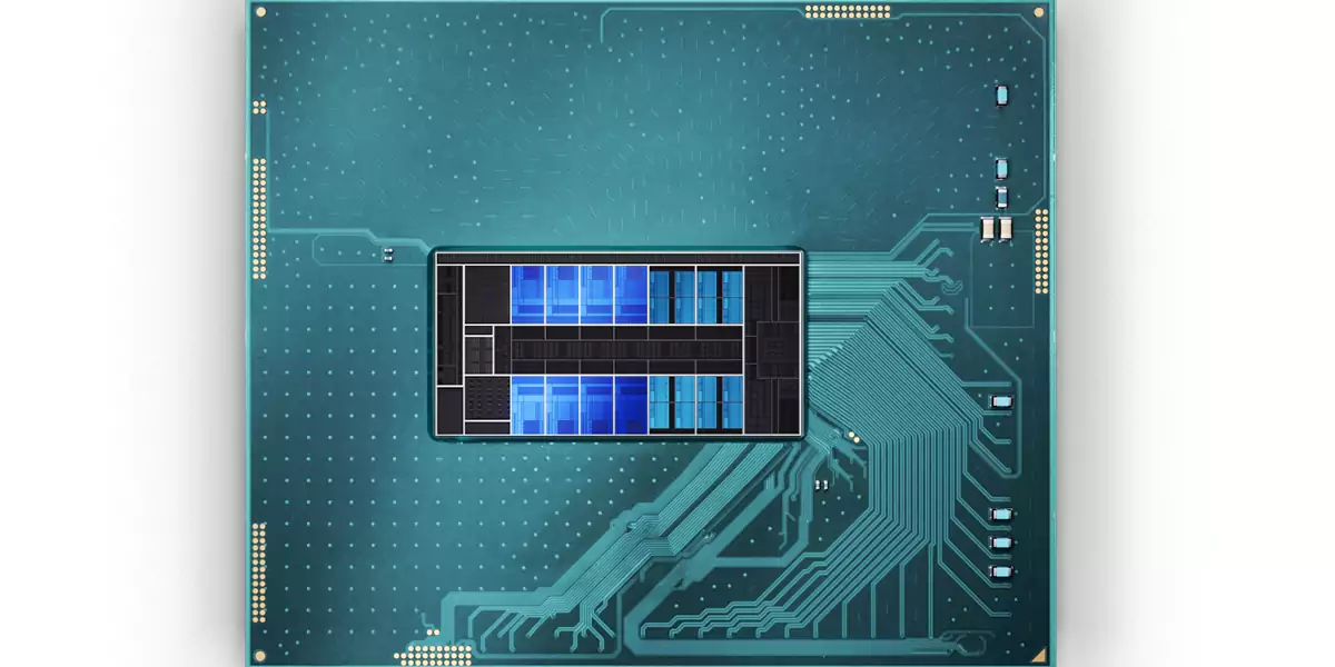
- PowerVIA Power Delivery: This technique involves placing power supply lines on the back of a chip, rather than the front.
This rearrangement not only improves power efficiency but also enhances overall chip performance. - Next-Gen Process Nodes: The development of next-generation process nodes is crucial in reducing transistor size.
This miniaturization will allow for a higher density of transistors within a chip. - 3D Chip Stacking: Another groundbreaking approach is 3D chip stacking. This technique involves interconnecting 16 or more integrated circuits vertically, enabling them to function as a single unit.
The Changing Economics of Chip Manufacturing
Gelsinger, as per the report, also highlights a shift in the economics of chip manufacturing.
The cost of building a modern fabrication plant (fab) has doubled in less than a decade, soaring from approximately $10 billion to $20 billion.
One can only hope Intel’s ambitions can keep up with the rising cost of semi-conductor manufacturing.
FAQs
What is Intel’s goal for 2030 in terms of chip development?
Intel has set an ambitious goal to develop a chip containing a trillion transistors by 2030. This initiative marks a major leap forward in semiconductor technology, moving beyond the traditional constraints of Moore’s Law.
How does “Super Moore’s Law” differ from the original Moore’s Law?
“Super Moore’s Law,” or “Moore’s Law 2.0,” as introduced by Intel’s CEO Pat Gelsinger, represents a more aggressive growth in transistor counts.
It aims to accelerate the pace of chip miniaturization and power beyond the original Moore’s Law, which suggested a doubling of transistors approximately every three years.
What role will TSMC and Samsung Foundry play in Intel’s chip development?
TSMC and Samsung Foundry are key collaborators with Intel in developing the trillion-transistor chip.
They will be instrumental in leveraging advanced 2nm node technology, crucial for achieving the high transistor count.
What are the innovative techniques Intel plans to use for its trillion-transistor chip?
Intel plans to employ several innovative techniques, including PowerVIA power delivery, next-gen process nodes, and 3D chip stacking.
These technologies are essential for increasing transistor density and improving chip performance.
Also Read: CES 2023- Intel announced its 13th Gen Intel Core Mobile Processors