To contribute towards the development of semiconductor sector in India, Vedanta, one of India’s leading multinational groups, and Taiwan-based electronics manufacturing company Hon Hai Technology Group (Foxconn), has recently signed a MoU to form a joint venture (JV) company that will manufacture semiconductors in India.
This is the first joint venture in the electronics manufacturing space after Prime Minister Narendra Modi approved the comprehensive program for the development of sustainable semiconductor and display ecosystem in India.
In December 2021, India had approved a comprehensive program for the development of sustainable semiconductor and display ecosystem in the country. Under the initiative, Rs76000 crore (>10 billion USD) approved for development of semiconductors and display manufacturing ecosystem in India.
According to the government, the program will usher in a new era in electronics manufacturing by providing a globally competitive incentive package to companies in semiconductors and display manufacturing as well as design. This shall pave the way for India’s technological leadership in these areas of strategic importance and economic self-reliance.
Vedanta and Foxconn collaboration
The collaboration between Vedanta and Foxconn follows the India Government’s recent policy announcement for Electronics Manufacturing & PLI scheme for incentivizing organizations to contribute towards development of this sector.
According to the MoU signed between the two companies, Vedanta will hold the majority of the equity in the JV, while Foxconn will be the minority shareholder. Vedanta chairman Anil Agarwal will be the chairman of the joint venture company.
“The targeted project plans to invest for manufacturing semiconductors. It will provide a significant boost to domestic manufacturing of electronics in India,” reads a statement issued by the Foxconn. The location of the plant is yet to be finalised. “Discussions are currently ongoing with a few State Governments to finalize the location of the plant,” it adds.
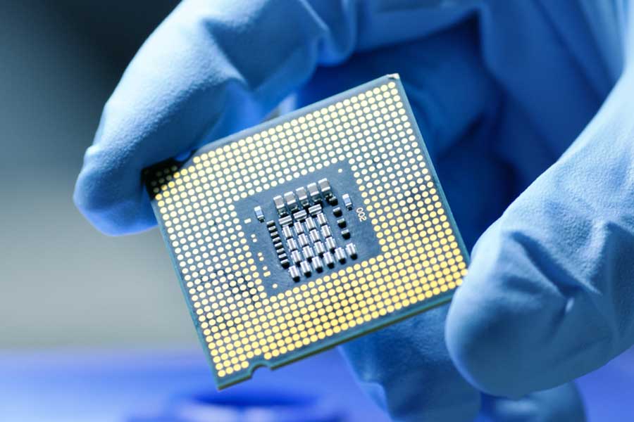
What is semicondutor
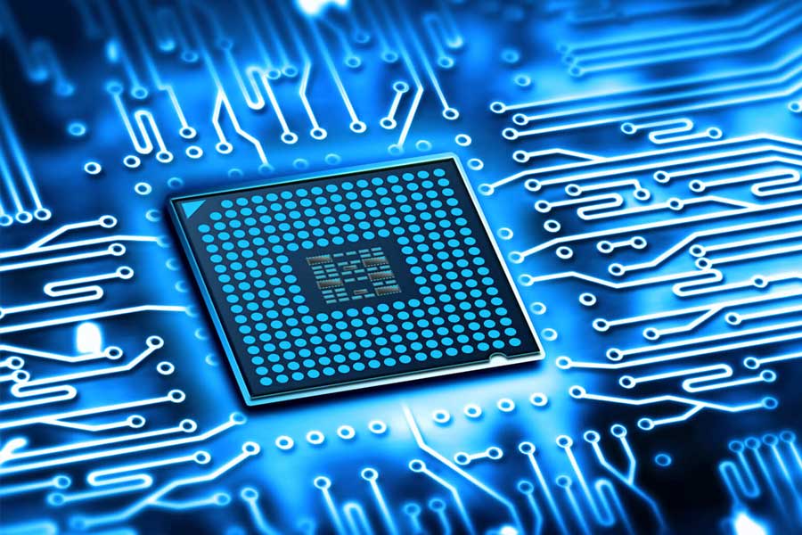
Government has described the semiconductors and displays as the foundation of modern electronics driving the next phase of digital transformation under Industry 4.0. Semiconductors and display manufacturing is very complex and technology-intensive sector involving huge capital investments, high risk, long gestation and payback periods, and rapid changes in technology, which require significant and sustained investments.
Here is the list of incentives approved by the government for the development of semiconductors and display manufacturing ecosystem in India:
Semiconductor Fabs and Display Fabs: The scheme for setting up of semiconductor fabs and display fabs in India shall extend fiscal support of up to 50% of project cost on pari-passu basis to applicants who are found eligible and have the technology as well as capacity to execute such highly capital intensive and resource incentive projects. Government will work closely with the state governments establish high-tech clusters with requisite infrastructure in terms of land, semiconductor grade water, high quality power, logistics and research ecosystem to approve applications for setting up at least two greenfield semiconductor Fabs and two Display Fabs in the country.
Semi-conductor Laboratory (SCL): Union Cabinet had also approved that Ministry of Electronics and Information Technology will take requisite steps for modernization and commercialization of Semi-conductor Laboratory (SCL). MeitY will explore the possibility for the Joint Venture of SCL with a commercial fab partner to modernize the brownfield fab facility.
Compound Semiconductors / Silicon Photonics / Sensors (including MEMS) Fabs and Semiconductor ATMP / OSAT Units: The scheme for setting up of Compound Semiconductors / Silicon Photonics / Sensors (including MEMS) Fabs and Semiconductor ATMP / OSAT facilities in India shall extend fiscal support of 30% of capital expenditure to approved units. At least 15 such units of Compound Semiconductors and Semiconductor Packaging are expected to be established with Government support under this scheme.
Semiconductor Design Companies: The Design Linked Incentive (DLI) Scheme shall extend product design linked incentive of up to 50% of eligible expenditure and product deployment linked incentive of 6% – 4% on net sales for five years. Support will be provided to 100 domestic companies of semiconductor design for Integrated Circuits (ICs), Chipsets, System on Chips (SoCs), Systems & IP Cores and semiconductor linked design and facilitating the growth of not less than 20 such companies which can achieve turnover of more than Rs.1500 crore in the coming five years.
India Semiconductor Mission: In order to drive the long-term strategies for developing a sustainable semiconductors and display ecosystem, a specialized and independent “India Semiconductor Mission (ISM)” will be set up. The India Semiconductor Mission will be led by global experts in semiconductor and display industry. It will act as the nodal agency for efficient and smooth implementation of the schemes on Semiconductors and Display ecosystem.
Fiscal support for semiconductors and electronics
Incentive support to the tune of Rs55,392 crore (7.5 billion USD) was also approved under PLI for Larges Scale Electronics Manufacturing, PLI for IT Hardware, SPECS Scheme and Modified Electronics Manufacturing Clusters (EMC 2.0) Scheme.
Industry reaction
Reacting to the JV between Vedanta and Foxconn, Amarpreet Singh, an experienced Electronics Manufacturing Industry professional, says in his Linked post that we are going to see many more similar news in the coming months. Singh further says that it will take some years before we actually witness the benefits of the new semiconductor policy by the government, but yes it is a good start.
In addition, PLI incentives to the quantum of Rs.98,000 crore (USD 13 billion) are approved for allied sectors comprising of ACC battery, auto components, telecom & networking products, solar PV modules and white goods. Overall, the Union government has committed support of Rs2,30,000 crore (USD 30 billion) to position India as global hub for electronics manufacturing with semiconductors as the foundational building block.
Development of semiconductor and display ecosystem will have a multiplier effect across different sectors of the economy with deeper integration to the global value chain. The program will promote higher domestic value addition in electronics manufacturing and will contribute significantly to achieving a USD 1 Trillion digital economy and a USD 5 Trillion GDP by 2025.
IIT Kanpur director, Abhay Karandikar had expressed hope that the program for development of semiconductors ecosystem in the country will help setup Semiconductor fabs and revitalize SCL. “This will certainly enable #India to become a global hub of electronics manufacturing. We look forward to an #AatmaNirbharBharat in #electronic manufacturing with innovative and #indigenous electronic products,” said Karandikar in a Facebook post on December 15, 2021.
Also, Read Here: IGear launches wireless keyboard and mouse combo KeyBee Pro to retro-style your desk


